How do we design chips that power everything, from satellites and electric vehicles to smartphones and medical devices?
How do billions of transistors fit onto a fingernail-sized wafer while becoming faster, cooler, and more efficient each year?
As India builds a world-class semiconductor ecosystem, who will design the next generation of processors, intelligent sensors, and integrated systems?
The global landscape for Electronics and Semiconductor Engineering is currently defined by significant strategic investment and acute talent demand, fueled by worldwide efforts to secure supply chains and accelerate advanced hardware innovation. The global scarcity of engineers with multidisciplinary skills is particularly pronounced in this sector, highlighting the Programmes strategic value. Professionals in this field are crucial for the design, verification, and testing of complex Integrated Circuits (ICs) that power everything from consumer electronics to advanced telecommunications and automotive technology.
The EST Programme builds strong foundations in electronics, semiconductor physics, digital and analog circuits, CMOS technology, VLSI design flows, embedded prototyping, hardware-software integration, and system-on-chip development. Organisations are seeking professionals who can integrate engineering depth with cross-domain fluency, connecting programming with psychology, data with design, cybersecurity with governance, and AI with ethics. WPU GŌA’s transdisciplinary learning model and TDP structure have been specifically designed to prepare students for this new world.
Through the EST Programme, you will learn to think like an engineer and design like an innovator, moving from circuit-level modelling to chip design pipelines, from transistor behaviour to system-level architectures, and from device physics to real-world applications. WPU GŌA’s transdisciplinary and industry-integrated learning model ensures that you are not just trained in technical domains, but are prepared for the ethical, economic, and geopolitical contexts of semiconductor engineering.
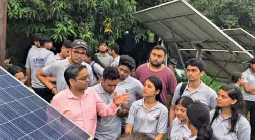
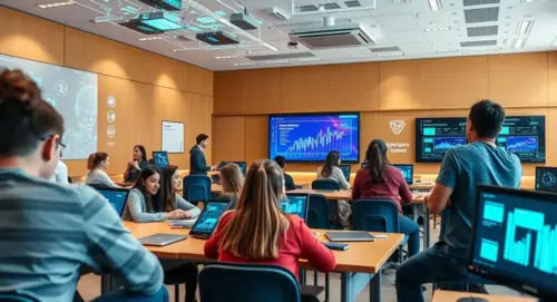
You will be taught by faculty who are researchers, semiconductor technologists, embedded engineers, materials scientists, and VLSI experts. Their work with industry, government missions, and research laboratories directly informs the curriculum. Through experiential learning, including advanced labs, makerspaces, EDA platforms, FPGA studios, field exposure, chip-design hackathons, and R&D mini-projects, you will develop the ability to translate ideas into high-performance systems.
Through research-driven pedagogy, labs, global immersions, national exposures, studio-based problem-solving, and a signature capstone, the EST Programme transforms students into engineers capable of shaping India’s and the world’s digital futures.